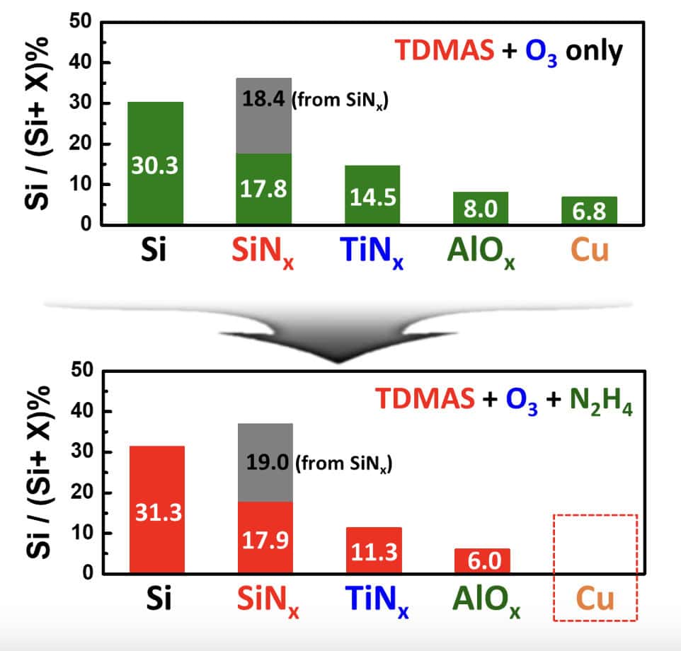
One of the challenges with continued device scaling is edge placement error (EPE) for the interconnect layers. One of the most effective integration approaches to reducing EPE involves using fully self-aligned Via formation using a dielectric-on-dielectric (DoD) deposition process. Typically, the self-assembled monolayer (SAM) is employed as a blocking layer for the subsequent ALD step. However, the degradation of the SAM and diffusion of the precursor beneath the SAM layer are two common drawbacks to this method. In this work, performed at UT Dallas, the use of anhydrous Hydrazine (N2H4) vapors, produced by RASIRC, was explored as a method to clean the Cu surface while also preventing dielectric from deposition on the Cu surface. This approach demonstrates the feasibility of improving the overall effectiveness of the self-aligned via integration scheme using dielectric on dielectric deposition.
