Tailoring crystallinity and polarity of GaN is of great interest to improving device performance in opto-electric devices, power devices operating at high voltage/temperature, and buffer layers for III-V semiconductors. However, conventional deposition techniques such as Metal Organic Chemical Vapor Deposition (MOCVD) Epitaxy, Molecular Beam Epitaxy (MBE), and Plasma Enhanced Atomic Layer Deposition (PE-ALD) and PE-CVD may not be suitable due to the first two techniques requiring extremely high temperature which leads to deformation during cooling due to thermal expansion coefficient mismatch, and PE-ALD/CVD embedding higher impurities from sputtered ligands. Therefore, developing a low temperature thermal ALD process is crucial in terms of both integration and achieving desirable film properties.
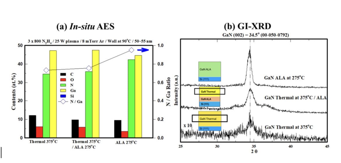
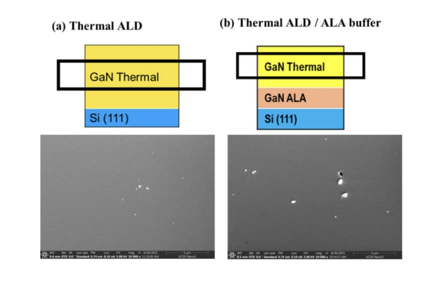
This work performed at UCSD employs Atomic Layer Annealing (ALA) technique where, in each cycle, GaN is deposited using tri(dimethylamino)gallium (TDMAGa) and hydrazine (N2H4, provided by RASIRC), integrated with a short Ar+ plasma anneal to deposit 30~40nm of GaN film on n-Si(111). ALD window was determined to be 275 to 425°C, with near stoichiometric Ga-N composition. Introducing Ar+ plasma annealing step after each deposition cycle resulted in drastic improvement in crystallinity, and film density, with decrease in O and C impurities. Additionally, ALA GaN exhibited mixed N and Ga-polar characteristics, while as-deposited GaN film possessed Ga-polar characteristics regardless of the presence of ALA GaN buffer layer beneath it.


